
Where Should Diamond Sit in a Chip's Thermal Path?
A system-level thermal-resistance framework for deciding where diamond particles, continuous spreaders and near-junction integration can create real value.
Diamond can reach exceptionally high thermal conductivity at room temperature. That has made it a natural candidate in discussions of advanced electronics cooling.
The immediate follow-up question should be: where exactly should it go?
Heat leaving a chip junction must pass through materials, interfaces, packaging, spreading structures, heat sinks or cold plates, and finally into air or coolant. Junction temperature is not determined by one material’s position in a conductivity ranking. It is determined by total resistance across that full heat-flow path.
That is the first principle I use when studying the diamond thermal-management industry: find where heat flow is most congested before looking for the material with the highest conductivity.
Draw the heat-flow path before evaluating diamond
A simplified chain from a heat-generating chip to the environment looks like this:
Junction → device material or substrate → interface → heat-spreading layer → package or heat sink → cold plate or cooler → environment
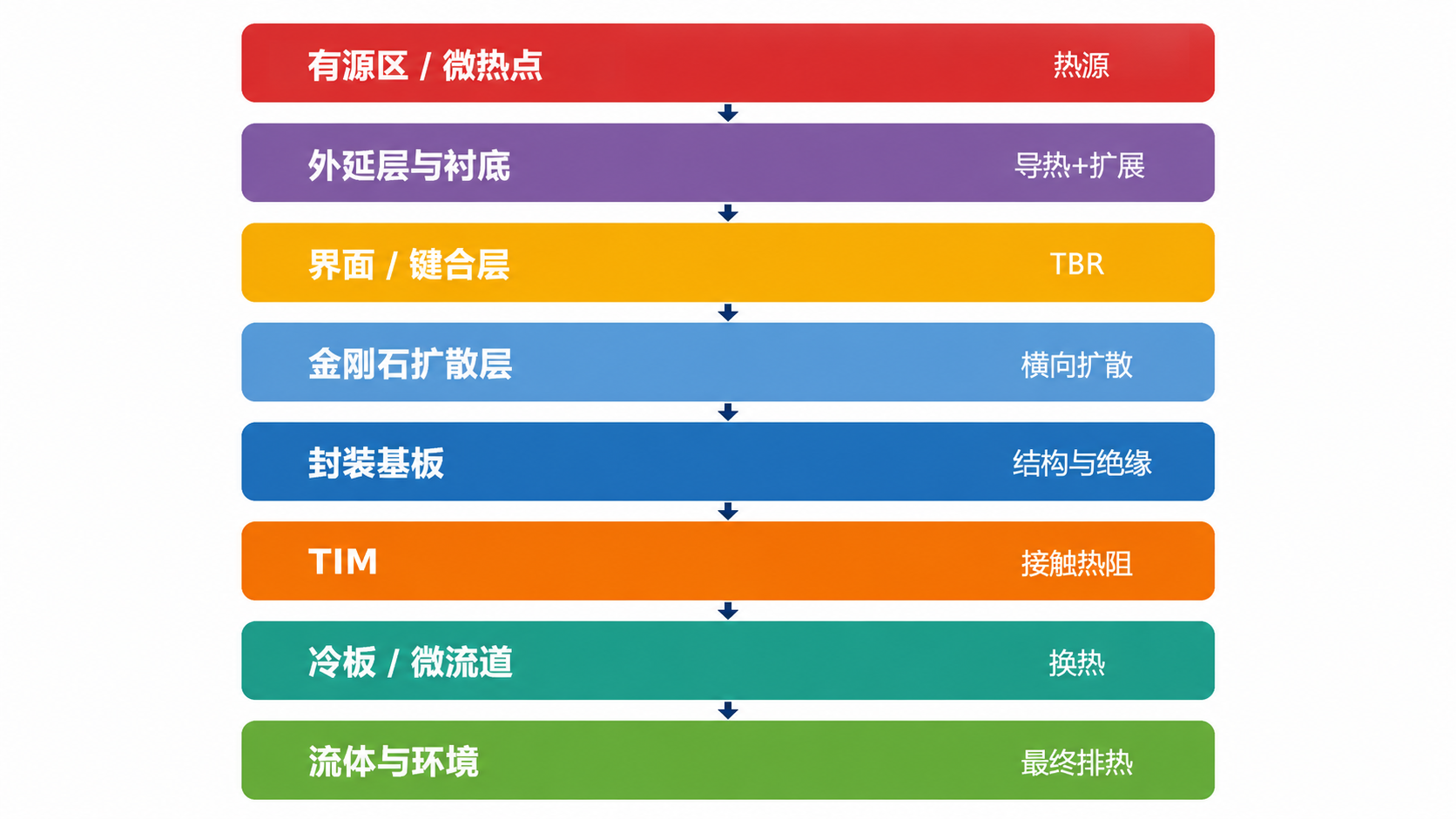
At least three forms of resistance appear along this chain.
Material resistance depends on thickness, area and thermal conductivity. It is the easiest term to compare and the one most often isolated in marketing.
Interface resistance arises wherever dissimilar materials meet. Even excellent bulk conductors can create a new bottleneck at a bonded or contacting surface.
Spreading resistance appears as heat moves from a small, high-flux source into a larger structure. The more concentrated the hotspot, the more consequential this resistance can become.
Together, they lead to a very different conclusion from a material ranking:
Cooling is not a contest between material properties. It is a network of thermal resistances.
High-conductivity diamond has economic value only when it can materially reduce the resistance currently dominating the system. If junction temperature is being set elsewhere, further increases in bulk conductivity produce diminishing system benefit.
When does diamond’s value increase?
The heat path suggests three practical questions.
Is the heat source a highly concentrated micro-hotspot? If heat is already distributed relatively evenly across a large area, conventional high-conductivity materials may be sufficient. Diamond becomes more compelling when local heat flux is so high that heat cannot spread laterally quickly enough.
Diamond is better suited to solving concentrated heat flow than simply a high temperature.
Is spreading resistance the current bottleneck? This is why a heat spreader is an important diamond product form. Its role is not merely to replace copper. It converts a small hotspot into a larger effective cooling area, changing heat distribution across the system rather than changing only one conductivity number.
Can the diamond be placed close to the heat source? Every additional layer between the hotspot and the diamond can dilute the material advantage. In principle, diamond gains leverage closer to the junction. The engineering and integration difficulty also rises at the same time.
Combined, those questions support a concise rule:
Diamond’s most valuable position is not necessarily the hottest point in the system. It is often the point where heat flow is most congested.
Three positions for diamond along the path
1. Diamond particles inside conventional thermal materials
Examples include diamond–copper, diamond–aluminium and polymer-matrix thermal composites. These products improve conduction and spreading within established package structures.
High particle conductivity does not guarantee equally high effective composite conductivity. Particle size, loading, interfacial bonding and wetting determine how much of the intrinsic advantage survives at product level.
2. A continuous diamond plate as a dedicated spreading layer
This group includes polycrystalline and single-crystal plates, ultrathin films, metallised diamond and diamond microchannel structures. It is better understood as a fast lane for redistributing heat than as another generic heat sink.
Its value comes from rapidly reducing local heat-flux density. Typical target applications include high-power lasers, power electronics and other modules with strongly concentrated heat loads.
3. Near-junction diamond integrated inside the device
GaN-on-diamond and related heterogeneous-integration routes place diamond much closer to the heat-generating junction. That positioning can translate material performance more directly into lower junction temperature.
It also introduces the hardest constraints: thermal boundary resistance, heterogeneous bonding, stress, wafer-scale processing, device reliability and long customer qualification cycles. At this level, a material problem quickly becomes a process, device and joint supplier-customer validation problem.
“Can diamond cool a chip?” is the wrong question
Three more precise questions matter:
- Where is the heat? What are the hotspot’s position, dimensions and heat flux?
- Where is the largest resistance? Is it the material, an interface, spreading resistance or downstream convection?
- Can diamond be placed there? Is integration technically feasible, manufacturable at scale and economically justified?
Once those questions are answered, diamond’s suitability becomes much more specific and realistic than the statement “thermal conductivity of 2,000 W/(m·K)”.
The more fundamental market question is therefore not how large diamond thermal management could become. It is: which part of the thermal resistance network are we asking diamond to remove?
Only then do market size, product route and industrial opportunity become meaningful. That is also why the underlying research separates the field by how diamond enters the thermal-management system: particle composites, continuous diamond plates or films, and near-junction routes such as GaN-on-diamond.
Continue the research
Evidence limits and uncertainties
- The dominant resistance in a real package depends on source geometry, material thickness, interface quality and boundary conditions; conductivity alone cannot identify it.
- Moving diamond closer to the junction may increase its thermal leverage, but also raises bonding, stress, wafer-process, reliability and qualification barriers.