
After Growing a 200 mm Diamond Crystal, What Must DF Still Prove?
Diamond Foundry's November disclosure showed a 200 mm single-crystal diamond in the as-grown, unpolished state. This article follows the disclosed route from heteroepitaxial seed and homoepitaxial ingot growth through slicing, finishing and integration, identifying the wafer-level quality and process evidence still needed before a deliverable substrate can be established.

At CarbonSemi 2026 in Ningbo, Diamond Foundry (DF) CEO Martin Roscheisen announced in a video presentation that the company had produced a 200 mm single-crystal diamond. On November 5, DF published a feature describing it as one continuous crystal, 200 mm in diameter, and showed photographs of the sample. DF’s announcement
For people working in MPCVD technology and production, the first question is often: is this an as-grown crystal, or a wafer ready for delivery? The caption beside the photograph answers half of that: the sample is “as-grown, unpolished.”
Rather than repeat the diameter, this article follows the production sequence to separate the newly disclosed route and equipment concepts from the process steps for which evidence is still missing.
1. The route: heteroepitaxial seed, homoepitaxial ingot growth
The presentation slides explicitly show a Si/YSZ/Ir structure. Si is silicon, YSZ is yttria-stabilized zirconia, and Ir is iridium. DF first builds a layered structure with an epitaxial orientation relationship on a non-diamond substrate. Bias-enhanced nucleation is then used to grow diamond with a controlled crystallographic orientation. The slides identify microwave plasma chemical vapor deposition, or MPCVD, as the diamond-growth method.
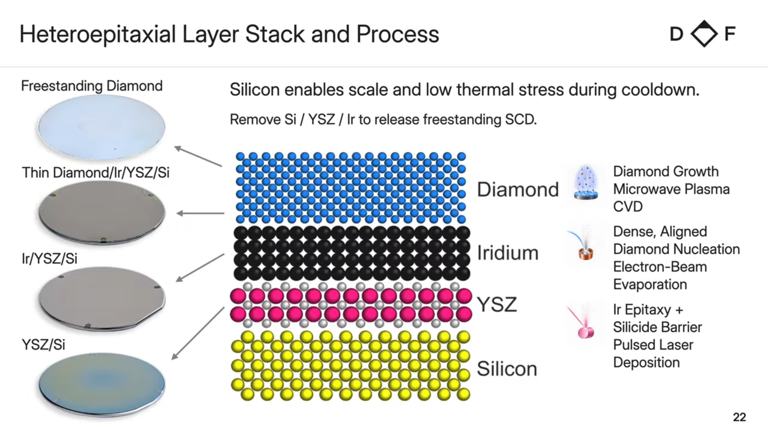
In the overall process shown by DF, silicon and buffer layers are removed to yield freestanding single-crystal diamond. A large-area seed is then used for homoepitaxial thickening into an ingot, followed by slicing and surface finishing before chip integration.
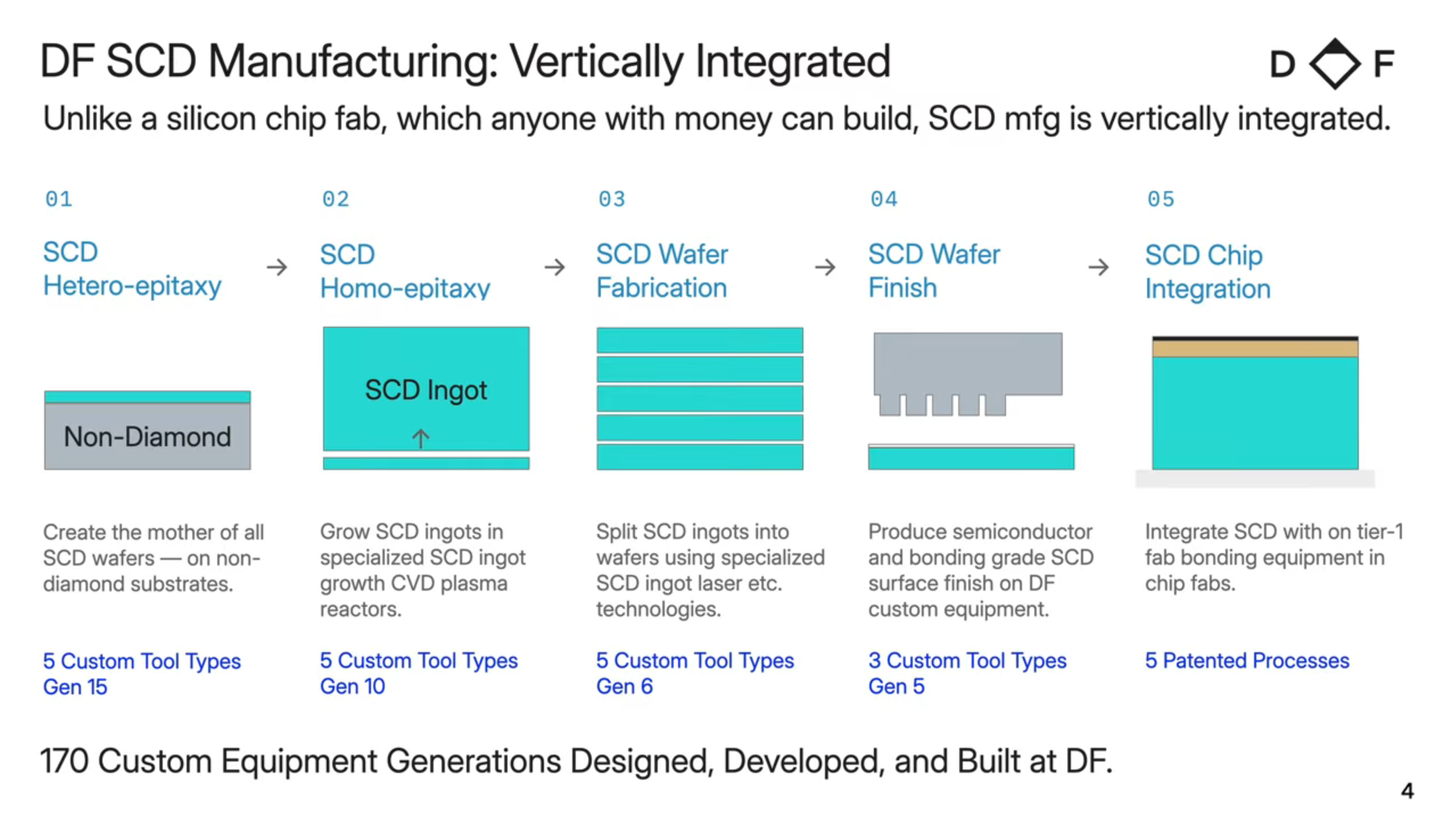
This route separates three problems: where a large-area seed comes from, how the ingot is thickened, and how slices become products. Seed area, growth quality and slicing yield are related, but each must be solved in its own right.
Heteroepitaxy is not new to DF this year; the presentation itself cites research from 2008 and 2017. What has changed in my view is that the company has placed its accumulated growth methods, ingot manufacturing, slicing and downstream integration into a more specific production sequence.
2. Device R&D sets material-quality targets
In earlier discussions of DF, I tended to view diamond MOSFETs as a longer-term route. In the nearer term, I focused more on combining diamond heat-spreading substrates with silicon chips and packaging.
The presentation adds another dimension. In the video, DF says it is developing substrates and diamond transistors in parallel so that actual devices can reveal which material properties matter, including the required dislocation levels.
That is practical for production. Tighter defect specifications often require more growth time and processing effort. How sensitive a device is to a given defect also depends on its structure and operating conditions. Feedback from devices can help materials and process teams connect improvements in crystal characterization to improvements in electrical performance, and identify process windows that matter in applications.
The slides show improvements in threshold-voltage and subthreshold-swing distributions, along with transistor characteristic curves. These company-reported results are worth tracking, but substrate dimensions, sample counts and yield definitions are still needed. They should not be treated as validation of a device array across a full 200 mm wafer. Device experiments can inform materials development; they do not by themselves establish commercial supply readiness.
3. Gen-10: judge the equipment by delivery metrics
The Gen-10 equipment in the presentation is 80 feet long, or about 24.4 meters. Its height is not specified; I estimate roughly 4 meters from the image proportions. The slide calls it a “single-crystal diamond ingot-growth cluster reactor,” and the photograph shows a row of repeated modules.
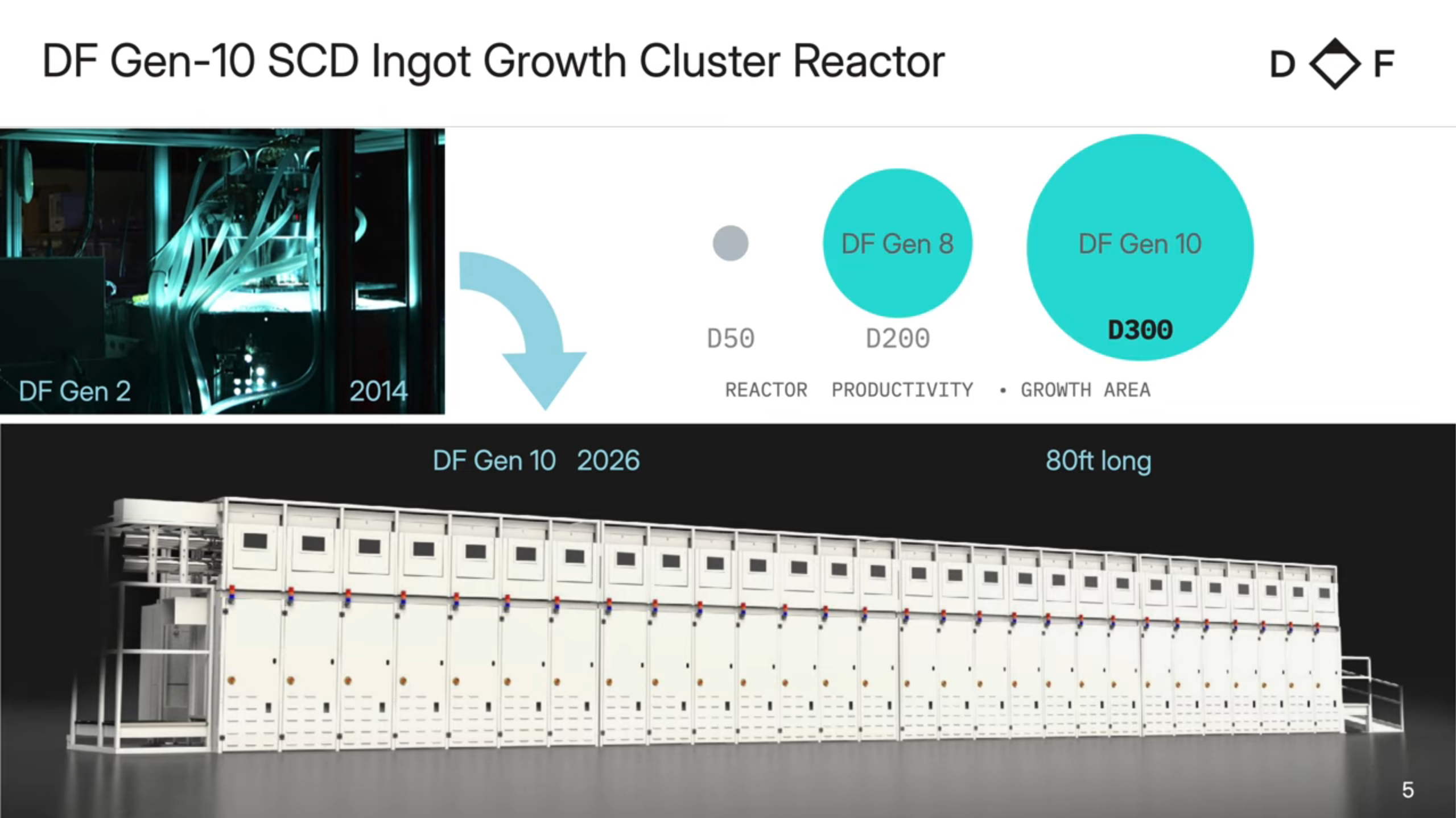
This shifts my attention from power and maximum growth diameter to the production platform as a whole: how processing area is increased, how parallel production is organized, how consistency is maintained among stations, and how the system connects with slicing and finishing. I see Gen-10 as an equipment concept aimed at semiconductor-material manufacturing. If demand for stable batch supply develops, parallel stations, modular controls and automation interfaces are likely to become important directions for MPCVD equipment.
However, the available photograph does not tell us whether it is a multi-station single chamber, a multi-chamber cluster, or a combination of several growth units. DF has not explained which microwave sources, vacuum systems, gas lines and temperature controls are independent or shared.
For semiconductor-material customers, equipment size ultimately has to translate into sustained delivery: how many spec-compliant substrates can be shipped each month, whether quality is consistent across stations and batches, and how much energy and processing cost each accepted part requires. These metrics say more about industrial progress than the dimensions of the equipment.
One more detail deserves caution. In the Gen-10 graphic, D300 appears under a “growth area” illustration. It may indicate growth-area development toward the 300 mm class, but the image is not evidence that DF has already produced a 300 mm single crystal.
4. The real boundary: quality of the 200 mm sample and downstream processing
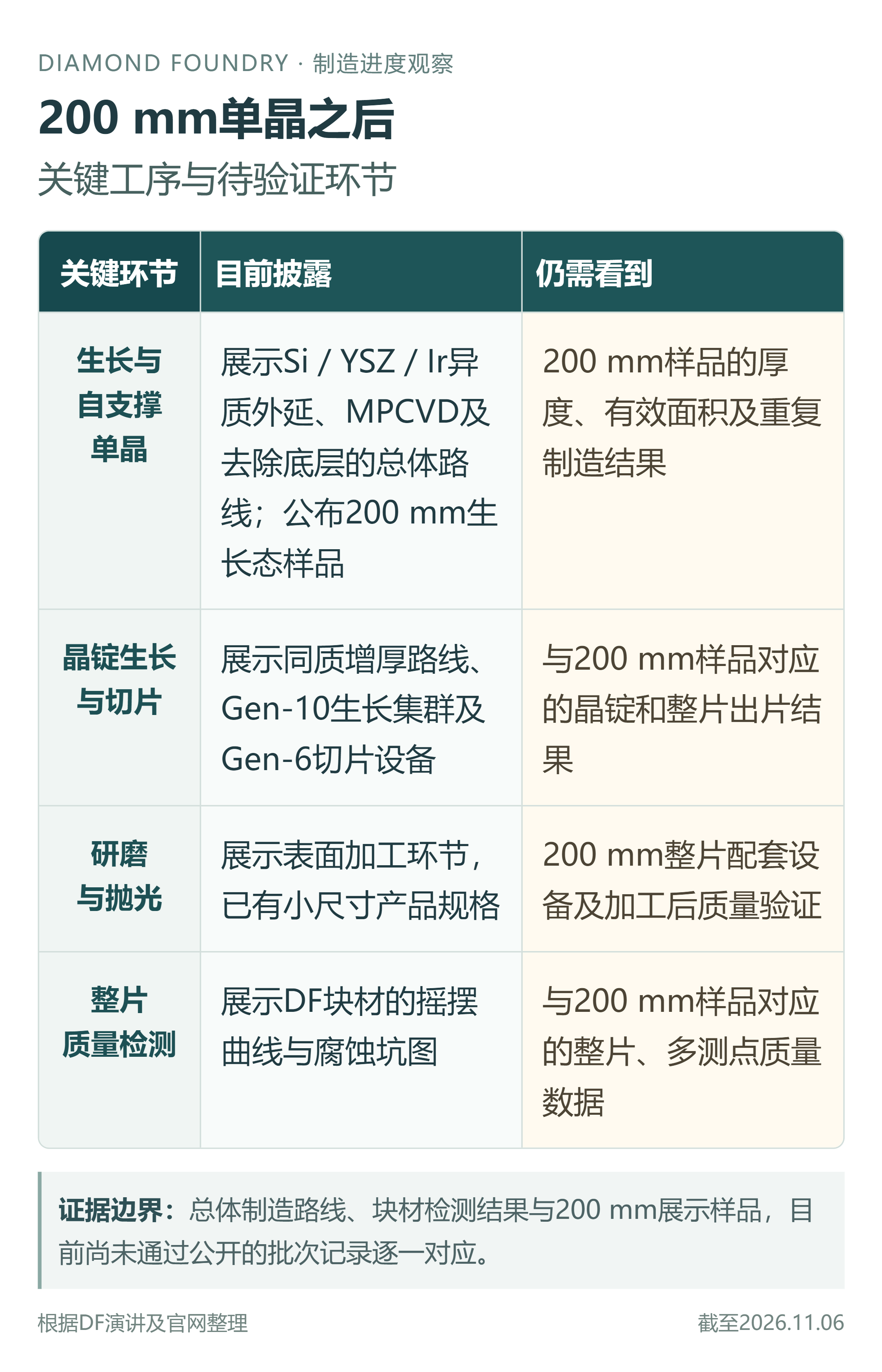
If we lay out the process DF disclosed as a production line, the knowns and gaps look roughly like this.
First, the quality evidence. The presentation does include crystal-quality data: rocking curves and etch-pit images, with an optimized full width at half maximum reported as 0.0094°. But that slide refers to DF bulk material. It does not say whether the measurement came from the same size or batch as the 200 mm sample, and it does not show a wafer-level quality map. One slide shows bulk-crystal quality; another shows a 200 mm object. Traceable measurement records are needed to connect the two.
I would like to see the 200 mm crystal’s thickness and usable area, center-to-edge distributions of orientation, defects and stress, and results from repeat growths. Point measurements and full-wafer uniformity determine what product can ultimately be made from it.
Next, can processing scale in step? DF’s exact description of the sample is “as-grown, unpolished.” The company has shown wafer-finishing steps and published specifications for smaller products, which indicates work on downstream processing. But that does not establish that the whole capability has been scaled to a 200 mm wafer.
It remains unclear whether 200 mm grinding, polishing and supporting equipment have completed validation at that diameter. The evidence needed is concrete: which equipment processes the full 200 mm piece; how much usable area remains afterward; how thickness variation, bow and surface damage are controlled; and whether multiple batches can meet the requirements repeatedly. Equipment that can physically accommodate a 200 mm sample is not the same as a stable process that produces a 200 mm substrate suitable for epitaxy or bonding. Process and metrology data still stand between them.
5. A timing detail
DF announced the development publicly in November, but the displayed sample may have existed by late September. I checked the capture information retained in the original JPEG on DF’s homepage: it records a shooting time of September 29, 2026, at 13:26 in UTC−7, which converts to the early hours of September 30 in Beijing. A separate image named D200 has a file-list date of October 1.
These clues support placing the sample’s existence as early as late September. But photo metadata can be changed, and a file-list date is no substitute for production records. The exact growth-completion date therefore remains unknown. Research should record “the sample existed” separately from “the company publicly announced it.”
6. Three things to watch next
This presentation makes me more inclined to track DF’s semiconductor manufacturing capability. It provides a more specific technical route than a size announcement alone and shows the links among materials, equipment and device R&D. I will focus on three questions:
- Will DF provide repeatable, multi-point quality data across the full 200 mm sample?
- Have 200 mm grinding, polishing and metrology been validated in step with growth?
- To what specifications will the first qualified products from this manufacturing chain be submitted for customer acceptance?
For others in the field, the useful benchmark is not a diameter in isolation, but the usable-area utilization and acceptance yield at every step of the chain.
Sources and method: This article draws on DF’s official CarbonSemi 2026 presentation video, a transcript and slide captures, as well as the 200 mm single-crystal announcement and technology-stack page. Claims about samples, performance and process progress are presented as company disclosures; the industrial analysis is the author’s. The image capture time is taken from metadata retained in DF’s original JPEG.
Evidence limits and uncertainties
- Public bulk-crystal quality data have not been traceably tied to the 200 mm sample by size, batch and wafer-level distribution.
- The Gen-10 image does not disclose reactor configuration or which microwave, vacuum, gas-flow and temperature-control systems are shared; appearance alone cannot establish throughput.
- DF describes the 200 mm sample as as-grown and unpolished; public evidence has not established same-diameter validation of full-wafer grinding, polishing, metrology or repeatable delivery.
Sources
- D200mm: A New Scale for Single-Crystal Diamond|Diamond Foundry
- CarbonSemi 2026 speaker announcement|EET China
- Diamond Foundry Technology Stack|Diamond Foundry
- CarbonSemi 2026 keynote video|Diamond Foundry / CarbonSemi 2026