
Diamond Foundry's Website Has Changed: Diamond Is Being Framed as a Chip Component Customers Can Specify
A comparison of Diamond Foundry's spring and October website snapshots shows a sharper focus on chip applications, a new Products entry, and defined 33 × 26 mm and 18 × 18 mm substrate offerings. Product specifications and supply language are more concrete, but they do not establish volume delivery, customer qualification or repeatable 200 mm manufacturing.
A return to DF six months later: what is now specified, and what remains unproven
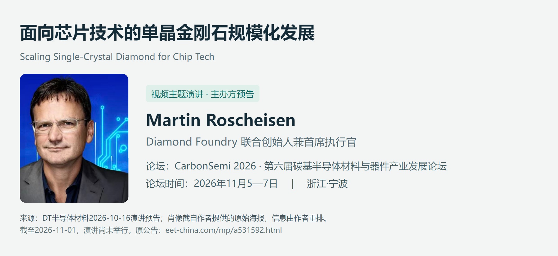
A speaker announcement for Diamond Foundry’s (DF) CEO recently prompted me to revisit the company’s website. According to the organizer, Martin Roscheisen is scheduled to deliver a video keynote, “Scaling Single-Crystal Diamond for Chip Tech,” at CarbonSemi 2026, the Sixth Forum on the Development of Carbon-Based Semiconductor Materials and Devices, in Ningbo on November 5–7. Speaker announcement
DF is not new to me. I completed a research report on the company in April and May. In June, while discussing the commercialization outlook for diamond MOSFETs with readers, someone asked whether DF’s semiconductor direction was a real business story. I was cautious: I was referring mainly to the route of using diamond itself as an active material to make transistors, and said that it was probably still a story. Seeing the keynote title made me ask a more specific question: what has DF made more concrete on the path toward chip technology? I compared its website with the materials I reviewed in the spring, looking at three things: what the site says, what the product pages offer, and where the evidence remains insufficient.
1. What the website says: from showing wafers to explaining chip applications
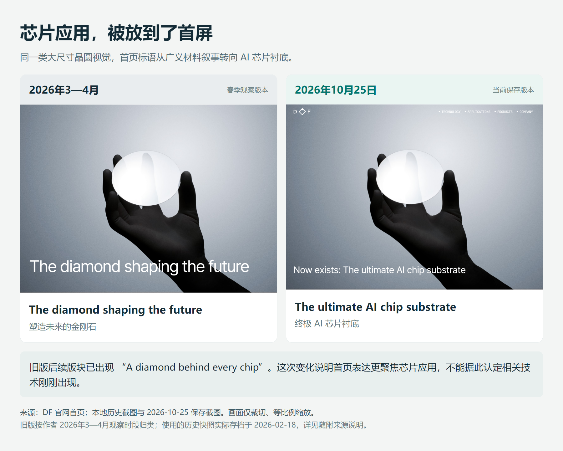
Start with the homepage. The spring baseline used the line “The diamond shaping the future,” and already included the idea of placing diamond behind every chip. The current first screen goes straight to “The ultimate AI chip substrate,” followed by language about hotspots, chip lifetime and application value. DF homepage Large wafers and technical milestones are still there; they have not disappeared. What has changed is that issues chip customers care about have moved into more prominent positions. The chip-application narrative existed in the spring, but is now organized more tightly and expressed in language closer to how customers use materials.
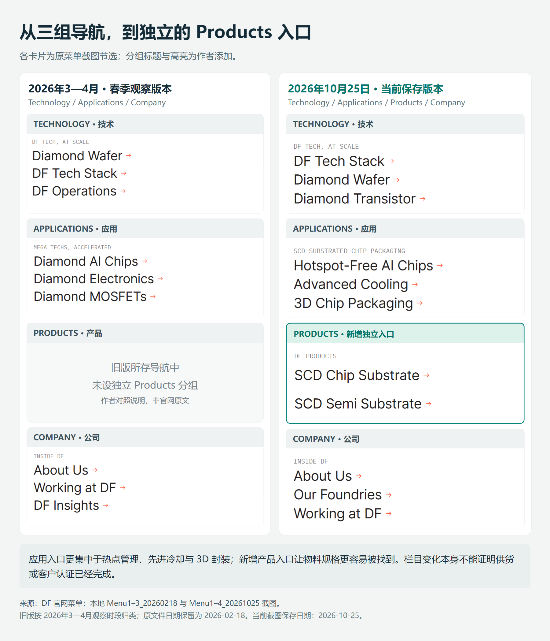
The navigation structure makes the shift clearer. The historical version was organized mainly under Technology, Applications and Company. The current site adds a top-level Products entry. Applications now prominently groups Hotspot-Free AI Chips, Advanced Cooling and 3D Chip Packaging. I read this sequence along the chip’s thermal path: where heat is generated, which interfaces it crosses, and how it is eventually removed. Thermal conductivity matters, of course. But DF’s explanation now gives more weight to where diamond sits, how it connects, and how the package is assembled.
2. What the website offers: product pages and supply language
The product pages make the change more tangible. They now show two single-crystal diamond offerings with defined dimensions: a 33 × 26 mm substrate aimed at chip companies, with specifications such as thickness, thermal-conductivity grade, total thickness variation and bow; and an 18 × 18 mm sample for R&D laboratories, positioned around surface conditions for device research and epitaxy. DF products Both are rectangular pieces. They should not be conflated with the full circular wafers shown on the homepage. Their significance is that customers can discuss procurement against specific dimensions, surfaces and delivery requirements. Material capability is being translated into requirements that can be checked one by one.
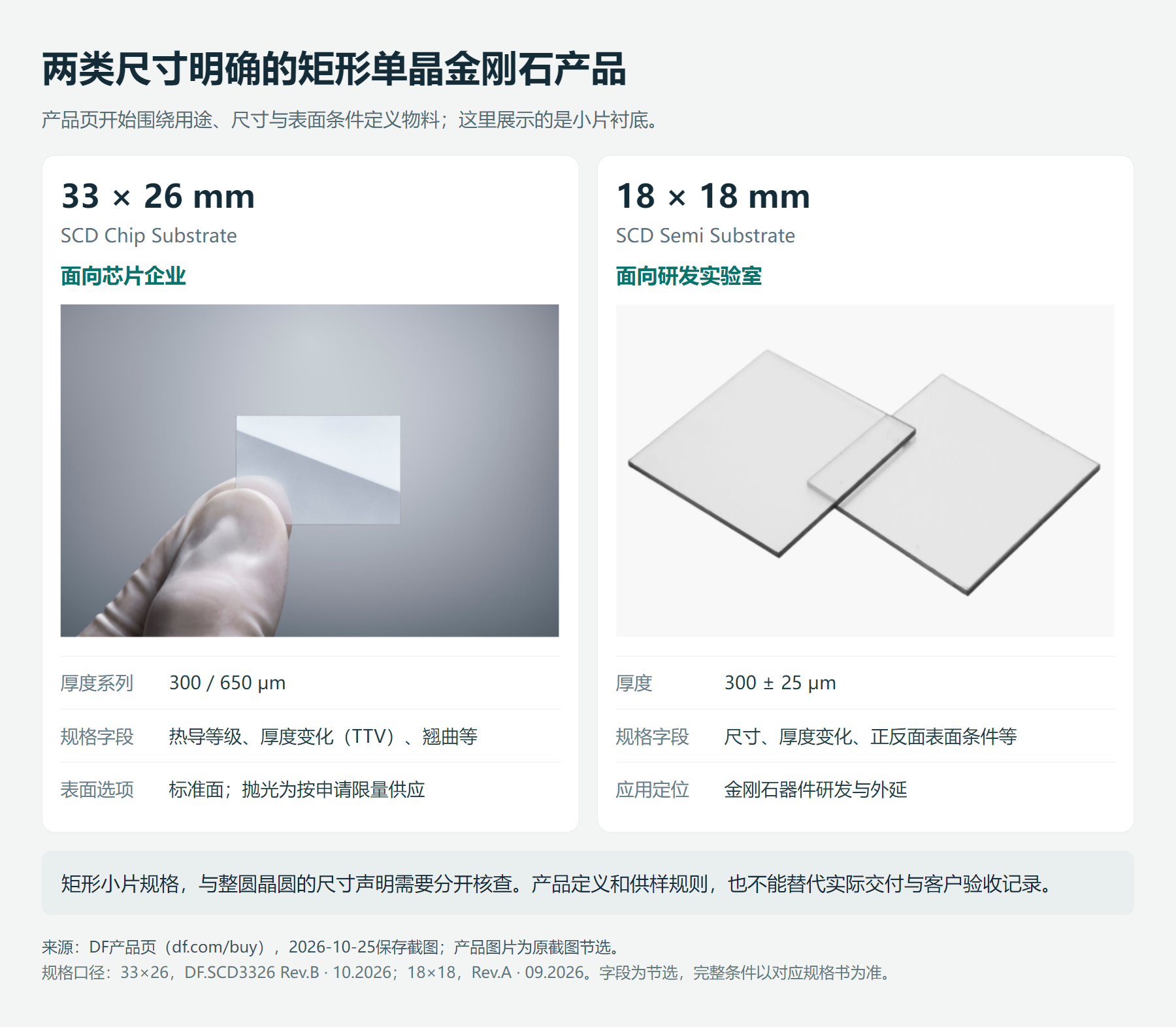
The supply language in the 33 × 26 datasheet is also quite specific: 25 pieces per lot, carrier packaging and a certificate of conformance for each piece. Surface options include a standard surface and a polished option available in limited quantities upon request; the two are not intended for exactly the same bonding approaches. 33 × 26 product datasheet These are familiar material and process-interface questions for semiconductor customers.
But I want to draw a boundary. Written supply rules do not mean that volume deliveries have already been completed. Nor should “supplying qualified chip companies” be read as proof that those customers have qualified DF’s products. Product specifications, actual sample supply, customer validation and recurring orders are separate evidence levels and need to be established separately. To me, the most interesting change is that DF’s website brings the discussion to this level: can diamond become an engineered component that customers can procure, process, integrate and qualify?
3. What the website does not clarify: 200 mm and performance multipliers
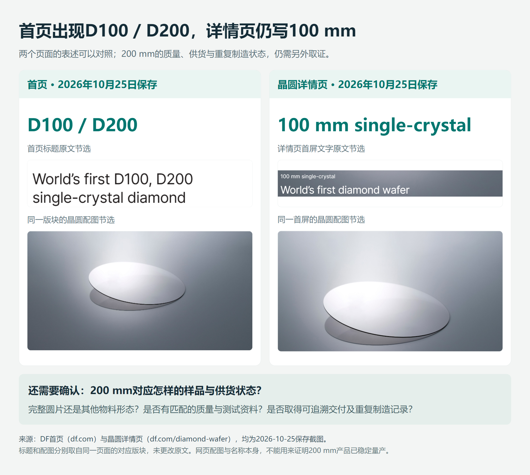
There are two areas where I cannot draw a conclusion. The first is the prominent D100 and D200 language on the homepage, while the wafer detail page still says 100 mm at the top. Those two pages alone do not tell me what samples, quality grade, supply status or repeatable manufacturing capability correspond to 200 mm. More evidence is needed to connect a product name or dimensional milestone to stable volume production. DF wafer page
The second is the large performance multipliers used in some cooling and packaging materials. They need to be assessed against the relevant test structure, model conditions and comparison baseline. A prominent number on a webpage cannot automatically be treated as a measured benefit for a product currently sold into a customer’s system.
4. My current view
In my spring report, I had already identified thermal-management interfaces as a near-term entry point and discussed bondable substrates and related experiments. This revisit adds a more concrete mapping to products and process steps, while making the remaining evidence gaps clearer. It also sharpens the distinction between the two routes we discussed in June: one uses diamond for heat spreading or packaging alongside existing silicon chips; the other uses diamond itself as the active transistor material. Their engineering tasks and commercialization hurdles differ, so they should not be judged on the same timeline.
My interim conclusion from this comparison is: DF’s public messaging is now more focused on chip applications, and its product and supply definitions are more specific. To assess whether its semiconductor business is taking shape, the key question is whether datasheets, experimental results and customer production lines can be tied to the same product, the same process and repeatable validation results.
I developed these questions further in the first installment of a Knowledge Planet series, “Diamond Foundry Semiconductor Productization: From Material Capability to Process Interfaces.” It examines what product specifications and supply rules reveal about maturity; what silver-sintering and surface-activated bonding experiments do and do not show; how reconstructed wafers might enter existing production lines; and what evidence is still needed between local demonstrations and customer qualification.
Evidence limits and uncertainties
- Public product pages and datasheets define offerings but do not by themselves establish volume delivery, customer qualification or recurring orders.
- The D100/D200 homepage language alongside a 100 mm wafer detail page does not establish the sample, quality grade, supply status or repeatability of a 200 mm product.
- Large performance multipliers in marketing materials require the corresponding test structure, model conditions and comparison baseline; they are not direct measurements of customer-system benefit.
Sources
- CarbonSemi 2026 speaker announcement|EET China
- Diamond Foundry|Diamond Foundry
- SCD Chip Substrate and SCD Semi Substrate|Diamond Foundry
- Diamond Wafer|Diamond Foundry
- SCD 33x26 Datasheet v11|Diamond Foundry